


What is it?
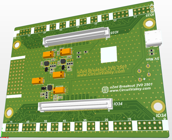
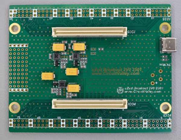
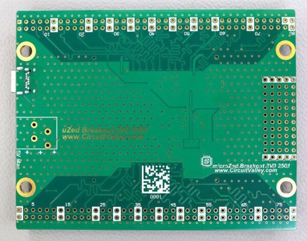
In this project, I set out to design a custom carrier PCB tailored for the MicroZed Zynq FPGA System-on-Module (SOM), inspired by the functionality of the AES-MBCC-BRK-G. Fully Open Project Eveything is available on github. PCB Design Schematic everything is available. This carrier board is designed to seamlessly interface with the MicroZed module, providing robust connectivity and enhanced peripheral integration for a variety of FPGA applications. From initial concept to detailed PCB layout, the design process focused on optimizing functionality, signal integrity, and scalability to suit custom project requirements. Whether you’re exploring embedded systems, hardware acceleration, or IoT development, this custom carrier board simplifies working with the powerful Zynq FPGA platform.
Why did you make it?
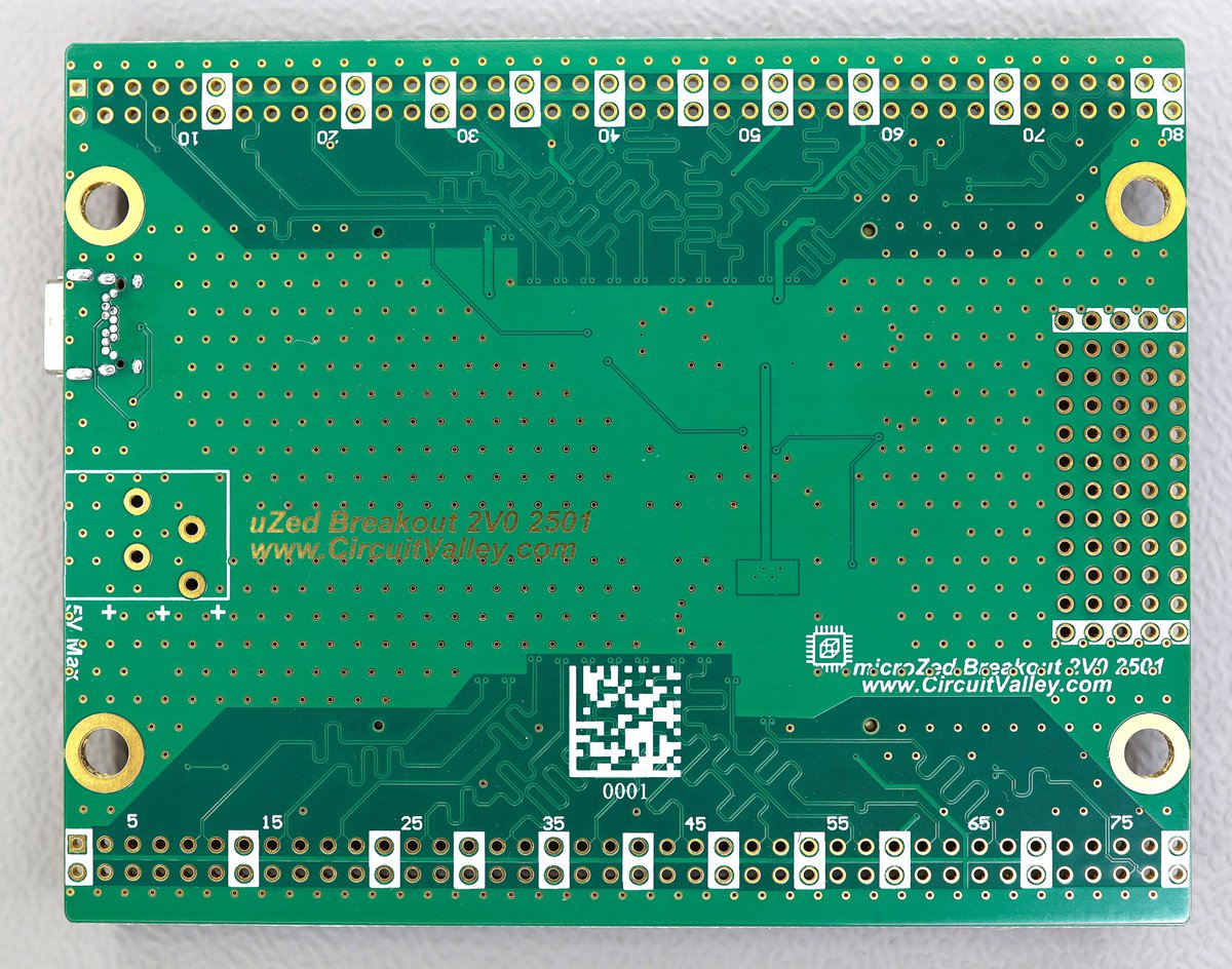
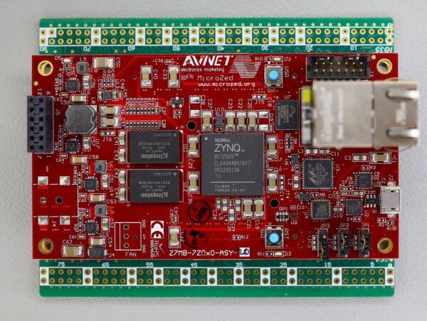
I will be using Avnet MicroZed Zync SOM board. But Avnet microZed Board has two 100 Pin fine pitch connectors for expansion, Which is impractical for prototyping so i decided to make my own breakout board. Finding Avent microzed GPIO breakout was little hard and official board has same VCCIO regulator for all banks and Avnet board also does not have differential LVDS layout.
What makes it special?
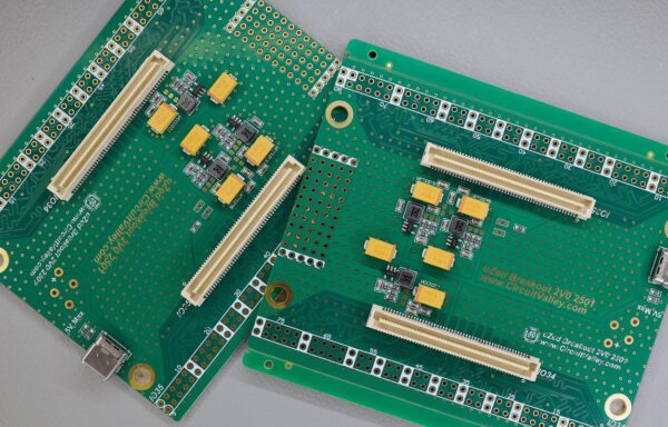
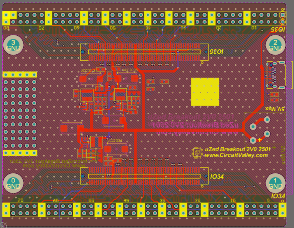
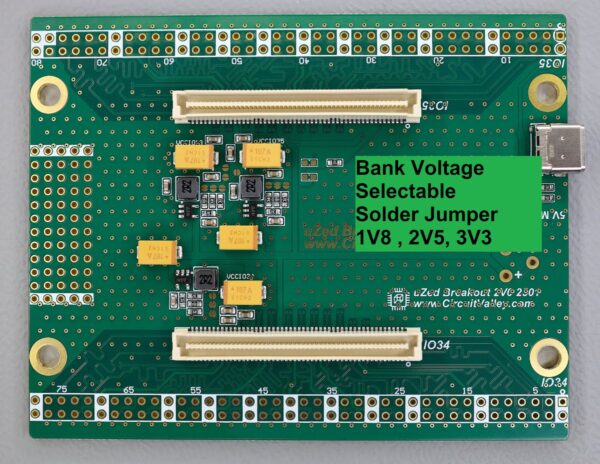
With three separate switching regulator for each bank VCCIO on 4 Layer Gold finish board with most of microZed pins broken out in LVDS pair. PCB is 4 Layer impedance control for 100R LVDS pair. Board has 3 solder jumpers per regulator to change bank voltage of each bank separately.

Reviews
There are no reviews yet.